
CASE STUDY
6 July 2026
Case study | Tommaso Salzillo, University of Bologna, July 2026
Using a 349 nm UV laser to characterise TIPS-pentacene organic semiconductor thin films
Researchers studying TIPS-pentacene organic semiconductor thin films used a 349 nm CW DPSS Skylark Laser as part of a Raman spectroscopy study investigating how thin-film processing affects crystal structure and molecular organisation.
TIPS-pentacene is used as a model organic semiconductor because its charge-transport properties depend strongly on how its molecules pack within a thin film. Identifying whether processing creates a different crystal form, changes molecular orientation, or alters film texture helps understand how manufacturing conditions relate to electronic performance.
The research combined UV Raman spectroscopy and grazing-incidence X-ray diffraction (GI-XRD) to distinguish between these effects in films deposited by bar-assisted meniscus shearing.
Confirming consistent crystal structure across processing conditions
The thin films were deposited at coating speeds ranging from 0.5 to 10 mm s⁻¹.
For the films produced at 10 mm s⁻¹, Raman spectra were collected using a Jobin Yvon T6400 triple-monochromator spectrometer with an Olympus BX40 confocal microscope and a 349 nm CW DPSS Skylark laser through a 20× LMU-NUV objective. Spectra were collected at several points on each sample to check reproducibility.
These measurements formed part of the wider comparison between films deposited at different coating speeds.
The Raman data showed that the deposited material retained the same Form I polymorph across the range of coating conditions studied. The authors concluded that the crystal structure remained invariant across a wide range of coating speeds, even though film texture and orientation were strongly developed during processing.
For device development, this suggests the processing window can be adjusted to control film alignment while retaining the same underlying crystal structure. This provides a cleaner route to optimising solution-processed TIPS-pentacene films for charge transport in devices such as OFETs, OLEDs and organic photovoltaics.
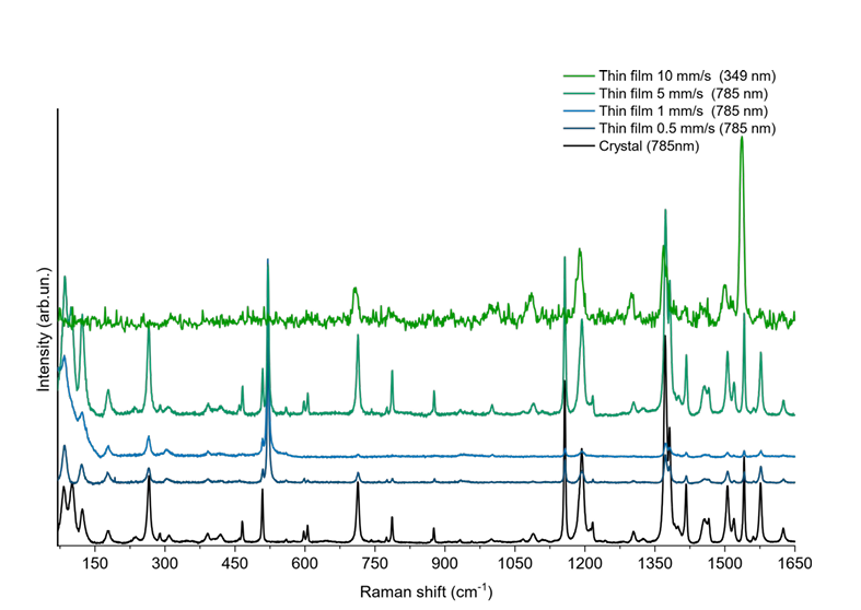
Fig. 1 Raman spectra of TIPS-pentacene films deposited at different coating speeds in the 50 1650 cm-1 wavenumber range. The spectra were acquired using 785 nm excitation, with the exception of the 10 mm/s film, for which a 349 nm excitation was used to compensate for the weak scattering expected from its lower thickness and to exploit resonance enhancement. The spectra confirm preservation of the Form I vibrational fingerprint in the series fabricated in the investigated BAMS conditions.
Connecting Raman fingerprints with molecular packing
The study also showed why Raman spectroscopy is useful for characterising organic semiconductor films.
The low-frequency spectrum contains modes associated strongly with molecular packing and lattice motion. Features around 81 and 122 cm⁻¹ were associated with non-totally symmetric lattice modes, while a feature around 30 cm⁻¹ was linked predominantly to intermolecular motion.
These vibrational fingerprints help distinguish between different possible crystal forms.
Calculations showed that different TIPS-pentacene crystal forms produce distinct Raman signatures because the molecules pack differently in each structure. Those packing differences also change the electronic interactions between neighbouring molecules, which can affect how efficiently charge moves through the material. Identifying the polymorph is therefore important for linking a measured Raman spectrum to the charge-transport behaviour expected from the semiconductor film.
From thin-film characterisation to organic electronic devices
Organic semiconductors are widely used in flexible, low-power electronic and optoelectronic devices, including OLEDs, organic photovoltaics (OPVs) and organic field-effect transistors (OFETs).
In these devices, performance depends strongly on how the molecules pack within the semiconductor film. Changes in crystal structure, molecular orientation and film texture can alter the electronic interactions that govern charge transport, including transfer integrals, reorganisation energies and dynamic disorder.
Thin-film characterisation is relevant to several established and emerging markets:
- OLED displays and lighting
- Organic photovoltaics and flexible solar cells
- Organic field-effect transistors (OFETs)
- Printed and flexible electronics
Conclusion
The practical challenge is that changing a coating process can affect several structural properties at once. A film may adopt a different polymorph, become more strongly textured or change its molecular orientation, and each of these can influence charge transport.
In this study, the researchers showed that films produced across a wide range of coating speeds retained the same Form I crystal structure while developing pronounced in-plane and out-of-plane texture. This separates changes in orientation from changes in polymorph and provides a clearer link between processing conditions, crystal structure and charge-transport behaviour.
For manufactures developing solution-processed organic semiconductors, that distinction is important when optimising coating processes for reproducible device performance.
This research is available to read at https://pubs.acs.org/aaoma6/article/4/7/2224/5200074/Disentangling-Polymorphism-Texture-and-Molecular