
CASE STUDY
9 June 2026
Case study | Grzegorz Staszczak, Institute of High Pressure Physics, Polish Academy of Sciences, June 2026
Using photoluminescence to understand semiconductor quantum structures
Researchers at the Institute of High Pressure Physics, Polish Academy of Sciences used a Skylark 320 DPSS laser for photoluminescence spectroscopy of InGaN/GaN quantum wells.
The study investigates how laser power density and hydrostatic pressure affect the built-in electric field and the Quantum-Confined Stark Effect (QCSE) in quantum wells with widths of 2.6 nm, 5.2 nm and 10.4 nm.
A key advantage of using the Skylark 320 was the ability to vary laser power density over approximately five orders of magnitude, making excitation intensity itself part of the experiment.
These effects are important in III-nitride semiconductor structures used in LEDs, laser diodes and other optoelectronic devices, because they influence both how efficiently electrons and holes recombine to produce light and the wavelength of the emitted light.
Probing carrier screening in InGaN/GaN quantum wells
In polar InGaN/GaN quantum wells, spontaneous and piezoelectric polarisation creates a built-in electric field that separates electron and hole wavefunctions.
This Quantum-Confined Stark Effect can reduce their overlap and influence both radiative recombination and emission energy.
For developers of III-nitride optoelectronic devices, these effects matter because the behaviour of the quantum well ultimately contributes to properties such as emission wavelength and light-generation efficiency.
The challenge becomes particularly important as InGaN technology is extended beyond established blue emitters towards green and red wavelengths, where higher indium content and stronger polarisation effects present additional difficulties.
By varying the 320 nm laser power density, the researchers could change the concentration of photo-generated carriers and measure how increasing carrier density progressively screened the built-in electric field.
Extending photoluminescence measurements with the Skylark 320 laser
The Skylark 320 laser provided the excitation intensity for this research.
- 320 nm excitation (3.87 eV): The excitation energy was above the bandgap of the quantum-well barriers and GaN substrate, enabling photoluminescence measurements of the InGaN/GaN structures.
- High laser power density: Focusing the beam to approximately 4.3 × 9.5 µm² produced an estimated maximum laser power density of around 114 kW/cm².
- Attenuable laser power density: Using an attenuator, the researchers varied laser power density from approximately 2 W/cm² to 10⁵ W/cm². This allowed the dependence of the photoluminescence spectra on laser power density to be studied across several orders of magnitude.
- Continuous wave operation: Continuous 320 nm excitation was used for both laser-power-dependent and hydrostatic-pressure-dependent photoluminescence measurements.
The combination of wavelength and available power allowed laser power density to be used as an experimental variable, enabling the investigation of carrier-dependent changes in the quantum wells rather than simply generate a PL signal.
Revealing carrier screening and new PL transitions with 320 nm excitation
The effect of increasing 320 nm excitation varied significantly with quantum-well width.
In the 2.6 nm quantum well, both ground-state and first excited-state transitions were observed across the excitation range, with their energies gradually increasing as laser power density increased.
The 5.2 nm quantum well showed a stronger dependence on excitation. Three electron-hole radiative recombination channels were identified, with the ground-state, first excited-state and second excited-state transitions appearing at progressively higher laser power densities. As the number of photo-generated carriers increased, the built-in field was increasingly screened and the observed transition energies changed.
The clearest demonstration came from the 10.4 nm quantum well. At low excitation, no photoluminescence was observed; PL emerged only above approximately 1 kW/cm² as carrier screening increased. At higher laser power densities, the measurements indicated almost complete screening of the Quantum-Confined Stark Effect. This was the most direct demonstration of the value of higher available 320 nm power in the experiment; allowing access different carrier-screening regimes and observe behaviour that was not present at lower excitation.
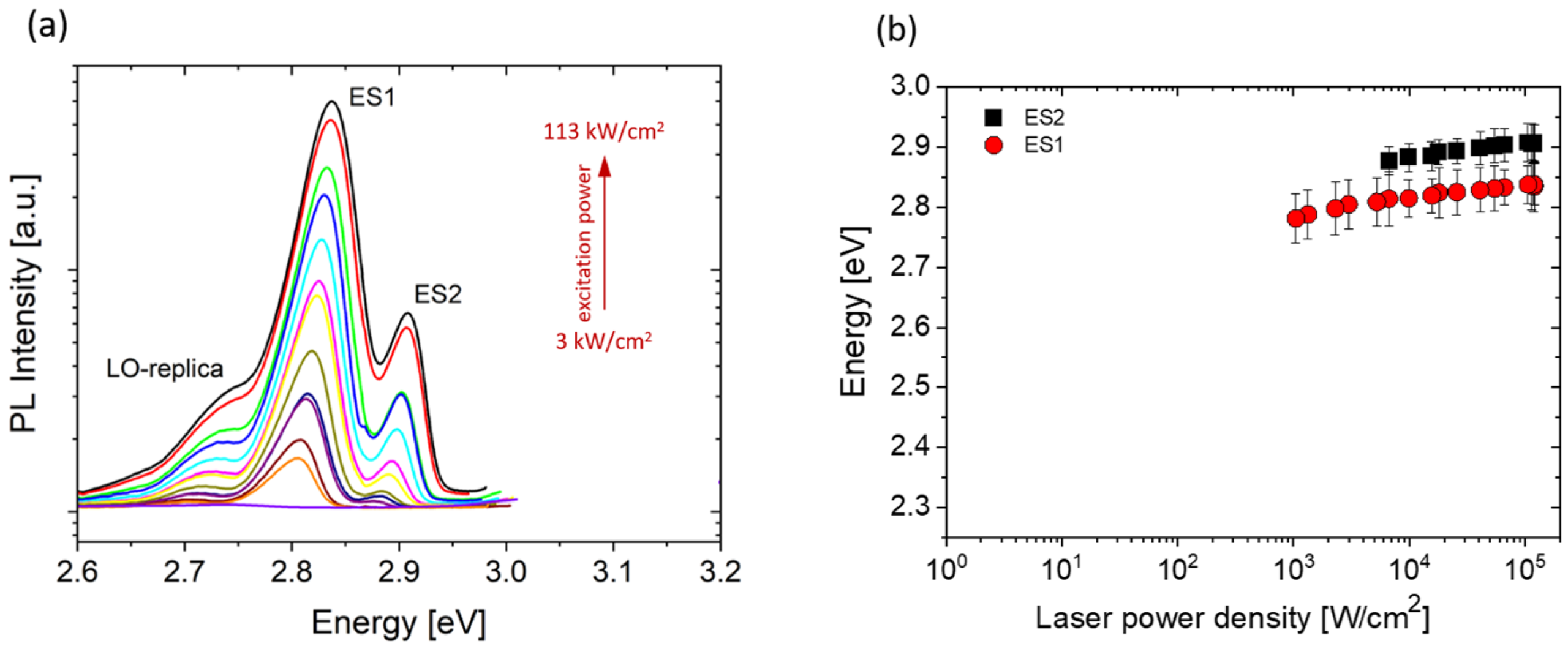
Fig. 1. (a) PL spectra for different excitation LPDs (starting from 3 kW/cm2 up to 113 kW/cm2) for sample C (10.4 nm well), (b) energy positions of two peaks versus LPD.
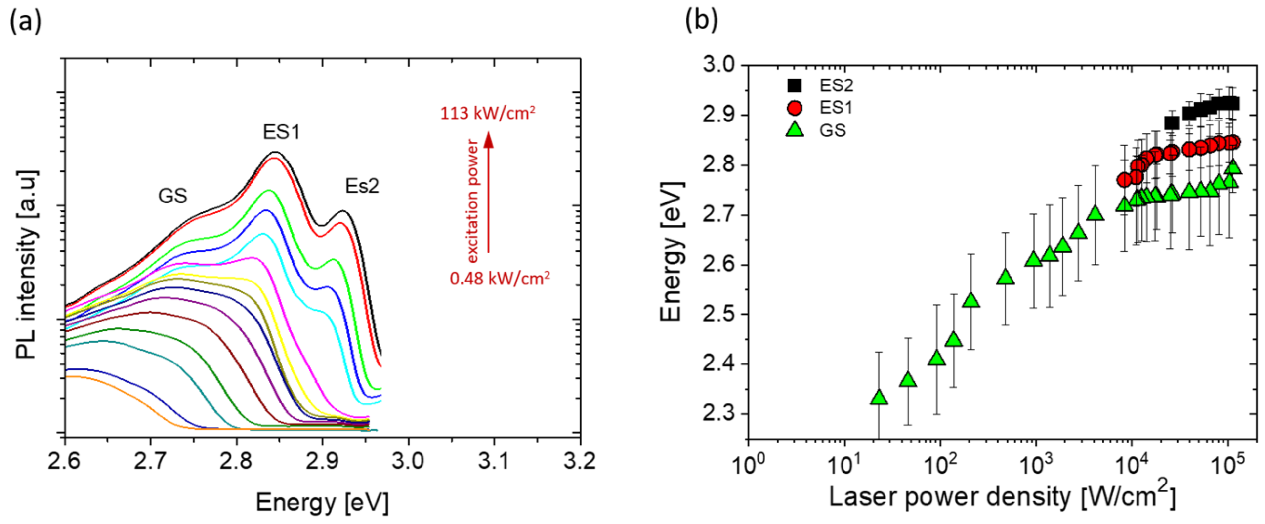
Fig. 2. (a) PL spectra for different excitation LPDs (starting from 0.48 kW/cm2 up to 113 kW/cm2) for sample B (5.2 nm well), (b) energy positions of three peaks versus LPD.
Combining laser excitation with hydrostatic pressure
The researchers also combined controlled 320 nm excitation with hydrostatic-pressure measurements up to approximately 4 GPa.
The two experimental variables act differently on the system: increasing carrier concentration screens the built-in electric field, while hydrostatic pressure increases it. Measuring the PL spectra as both parameters were varied allowed the team to examine these competing effects within the same quantum-well structures.
Pressure coefficients of the PL emission were used to investigate the evolution of the electric field. At high excitation levels, the values measured for the wider quantum wells approached those of bulk In₀.₁₇Ga₀.₈₃N, consistent with strong or almost complete screening of the built-in field.
From semiconductor spectroscopy to device development
Research of this kind supports the characterisation and development of materials used in solid-state lighting, displays, microLEDs, laser projection, automotive lighting, optical data storage and communications.
For the development of GaN and InGaN materials, quantum wells, and wide-bandgap semiconductor devices, the Skylark 320 provides high power 320 nm photoluminescence excitation where laser power density can be used not only to generate signal, but also as a controlled probe of carrier-dependent semiconductor behaviour.